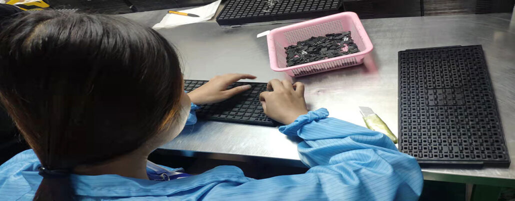
Process 1: Chip inspection. Purpose To check the overall appearance of the supplied chips.
Process 2: Planting solder paste.The solder paste machine will plant solder paste on the PCB where the chip needs to be soldered. The role of solder paste assists the chip to be pasted on the PCB.
Process 3: AOI inspection.Determine whether the solder paste scraping place on the PCB is defective
Process 4: Solder paste thickness inspection.Workers also check whether the thickness of the solder paste on each part of the PCB is uniform, and the products with problems will be selected immediately to avoid entering the next production link.
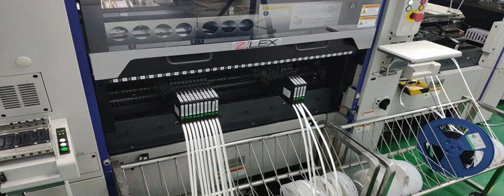
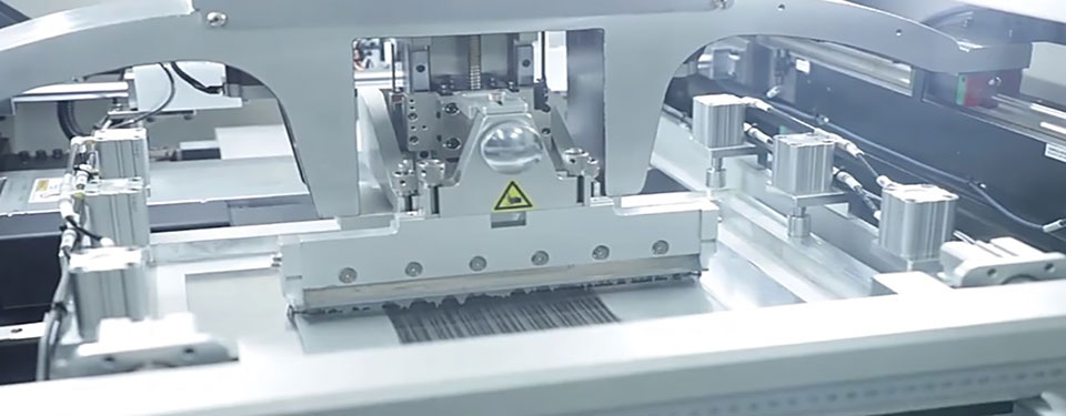
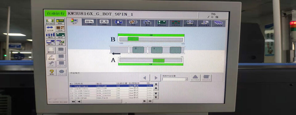
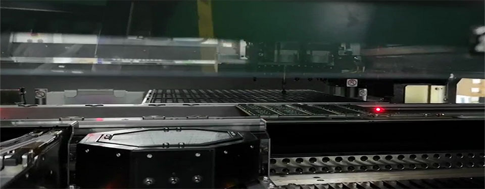
Process 5: SMT patch.The next step is to install memory chips, SPD (serial presence detection) chips and other components on the PCB
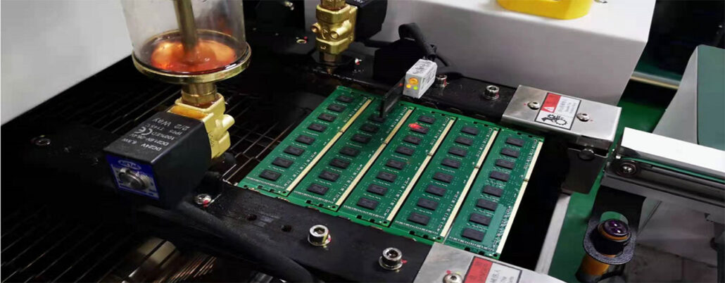
Process 6: Reflow soldering.After the components are adhered to the memory PCB by solder paste, they must be soldered by reflow soldering so that they can be fixed on the PCB.
Process 7: X-ray inspection.After reflow soldering, the memory is basically formed. The next step is to test. First, use an X-ray machine to detect the solder balls of the BGA (Ball Grid Array) package or WLCSP (Wafer Level Chip Package) memory chip to see if the soldering is normal.
Process 8:Visual inspection.After the X-ray inspection, a comprehensive and detailed appearance inspection of the entire memory PCB is carried out. This process is carried out by a worker visually under a magnifying glass.
Process 9: Labeling.After passing the visual inspection, the memory will enter the automatic labeling process, and the automatic labeling machine will automatically paste the product barcode on each memory module. The bar code mainly records the material number of the memory module, production serial number, product specifications, etc.
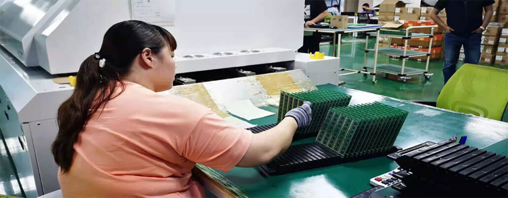
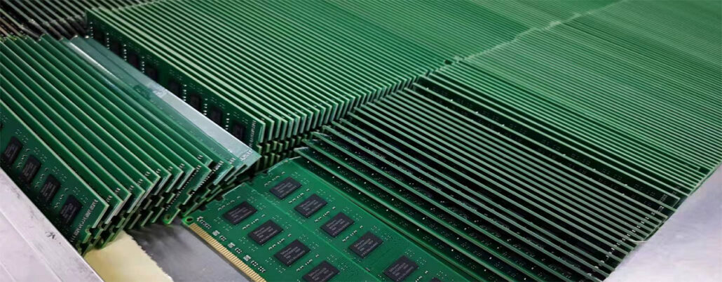
Process 10: Automatic cutting.Since the memory modules are produced in the form of on-board, the marked on-board memory modules must be divided into a single memory module by an automatic cutting machine, that is, the single memory module we usually see.
Process 11:Write SPD information.We know that generally there is an SPD chip on each memory stick, which records the operating frequency, operating voltage, speed, capacity and other information of the memory stick. Therefore, each memory stick that has been cut enters the SPD information writing process.

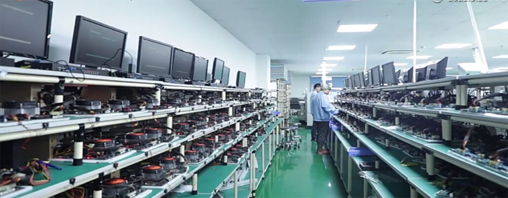
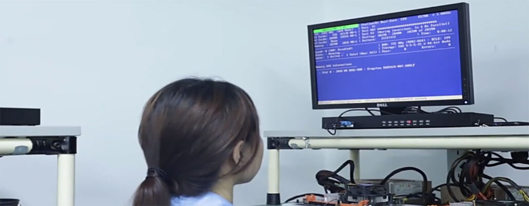
Process 12: Function test.Then the workers began to perform detailed and strict functional tests on the memory sticks. Test items include capacity, SPD information, data access, etc.
Process 13: Final visual inspection.After the test is completed, the memory module must pass the last appearance inspection
Process 14: Sampling inspection.The memory is also subject to random inspection.
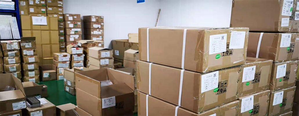
Process 15: Packing and warehousing.After passing the sampling test, we will seal the box and store it in the warehouse, waiting for shipment.
Process summary:Chip inspection →Planting Solder paste → AOI inspection → Solder paste thickness inspection → SMT patch → Reflow soldering → X-ray inspection → Visual inspection → Labeling → Automatic cutting → Write SPD information → Function test → Final visual inspection → Packaging → Sampling inspection → Packing and warehousing
Welcome to consult WHALEKOM’s products, we will give you feedback with superior quality and good after-sales service.